History
Includes the device achievement of Oki Electric Industry Co., Ltd. and OKI SEMICONDUCTOR CO., LTD. which are the predecessor of LAPIS Semiconductor Co., Ltd.
- 1960
∼ 1980 - 1980
∼ 2000 - 2000
∼
| Time | Genre | Article |
|---|---|---|
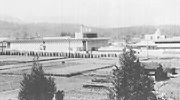
| 1961 | Facilities | Building No.1 completed
|
| Products | Production of transistors
|
|
| 1962 | Facilities | Building No.2 and No.3 completed
|
| Products | Production of millimeter wave
tubes and electronic computers 
|
|
| 1965 | Products | Production of reed relays /
Development of ICs started 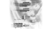
|
| 1966 | Products | Production of reed switches
|
| 1967 | Products | Production of ICs
|
| 1968 | Products | Development CMOS ICs started
|
| 1969 | Facilities | Building No.4 completed
|
| Products | Production of printed circuit boards
|
|
| 1975 | Facilities | (Operations begun at Chichibu plant)
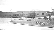
Chichibu plant |
| Products | Production of 4Kb DRAM
|
|
| 1977 | Facilities | VLSI Laboratory No.1 completed
|
| Products | Production of microprocessors
|
|
| 1979 | Products | Production of microcomputers
|
| Time | Genre | Article |
|---|---|---|
| 1980 | Facilities | Administration/Technology Center completed
|
| 1981 | Facilities | (Operations begun at Miyazaki Oki Electric)
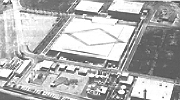
M1 Plant at Miyazaki Oki Electric |
| Products | Production of gate arrays and 64kb DRAMs
(3µm design rules used) |
|
| 1982 | Technologies | Technology transfer to National Semiconductor Inc.
|
| 1983 | Facilities | VLSI Laboratory No.2 completed
|
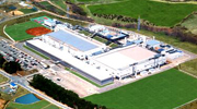
| Facilities | (M2 Plant completed at Miyazaki Oki Electric)
M2 Plant at Miyazaki Oki Electric |
|
| 1984 | Facilities | (Oki Micro Design Miyazaki established)
|
| Products | Production of 256kb DRAMs
(2µm design rules used) |
|
| 1985 | Facilities | VLSI Laboratory No.3 completed
|
| 1987 | Products | Production of 1Mb DRAMs
(1.2µm design rules used) |
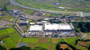
| 1988 | Facilities | (Operations begun at Miyagi Oki Electric)
Miyazaki Oki Electric |
| 1989 | Facilities | Production of 4Mb DRAMs
(0.8µm design rules used) |
| 1990 | Facilities | (Operation begun at Oregon Plant in U.S.)
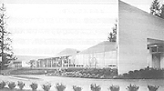
Oregon Plant |
| Facilities | (Oki LSI Technology Kansai established)
|
|
| 1991 | Facilities | (M3 Plant completed at Miyazaki Oki Electric)
|
| 1992 | Facilities | (Operations begun at Thailand Plant)
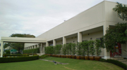
Thailand Plant |
| Facilities | ULSI Laboratory No.1 completed
|
|
| Products | Production of 16 Mb DRAMs (0.5µm design rules used)
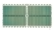
16M DRAM Pattern |
|
| 1994 | Products | 256Mb DRAMs (0.25µm design rules used)
successfully developed |
| 1995 | Facilities | (S2 Plant completed at Miyazaki Oki Electric)
|
| Products | Production of SSD cards
|
|
| 1996 | Facilities | New Cafeteria Building completed (Building No.6)
|
| 1997 | Facilities | New Administration/Technology Center completed
(Building No.7) |
| Products | Production of 64Mb DRAMs
(0.3µm design rules used) |
|
| Products | 1Gb DRAMs (0.18µm design rules used)
successfully developed |
|
| 1998 | Products | Business based SPA started
|
| Products | Surface-mount Optical Network Modules commercialized
|
|
| Products | USB Control LSIs commercialized
|
| Time | Genre | Article |
|---|---|---|
| 2000 | Products | Bluetooth System LSIs commercialized
|
| Products | µPLAT developed
|
|
| 2002 | Products | Production of LSIs using Fully
Depleted SOI-CMOS technology |
| 2003 | Products | Long-Wave Time Code Receiver based on
SOI-CMOS technology successfully developed, an industry first |
| 2004 | Facilities | Semiconductor Bases in Shenzhen, Beijing
and Shanghai established |
| 2005 | Facilities | Semiconductor Business Group established
|
| 2007 | Facilities | Silicon Microdevice Company established
|
| 2008 | Facilities | OKI SEMICONDUCTOR CO.,LTD. established |
| 2011 | Facilities | The company name changed to
LAPIS Semiconductor Co., Ltd.  |
| 2013 | Facilities | Moved the headquarter office at Shin-Yokohama.
 |
| 2015 | Products | Production of Reference design for IoT:Lazurite
|
| Products | Development of Soil Sensor
|
|
| 2017 | Products | Commercialization of Low Power Wide Area Transceiver LSI
|
| 2020 | Facilities | Absorbed and merged LAPIS Semiconductor Miyazaki and LAPIS Semiconductor Miyagi
Spun out of LSI development as LAPIS Technology Co., Ltd. |