Technologies to which LAPIS Semiconductor Miyazaki allocates resources
LAPIS Semiconductor Miyazaki focuses on unique technologies and responds to customer needs
Products
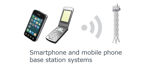
RFiCs (Radio frequency integrated circuits)
Application
Smartphones and mobile phone base station systems
Products
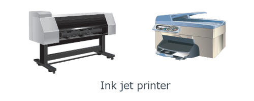
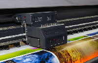
Piezo actuator products
Application
Ink jet printer
Silicon On Sapphire technology
Leading supplier of high quality CMOS for RF device by SOS wafers
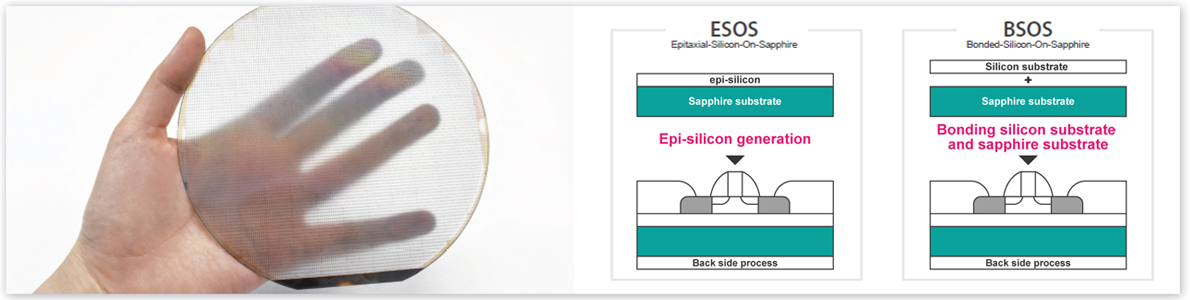
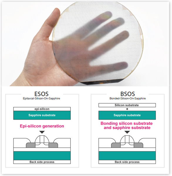
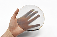
Two types of substrates: ESOS and BSOS
LAPIS Semiconductor Miyazaki manufactures SOS products using two types of substrates: ESOS that epi-silicon is generated on sapphire substrate, BSOS that silicon substrate is bonded to sapphire substrate.
Since these substrates are transparent as shown in the above, it is necessary to treat the back side so that process equipment can correctly recognize the presence of wafers and also implement electrostatic chuck.
High speed, high frequency characteristics, and low power consumption
SOS products are superior to silicon substrate products in terms of high speed, high frequency characteristics,
and low power consumption, and are applied to smartphone and mobile phone base station systems that transmit a large amount of information.
Application
Micro Electro Mechanical Systems technology
Thin film piezo ink jet head is applied to high-performance inkjet printer, which provides high-definition printing
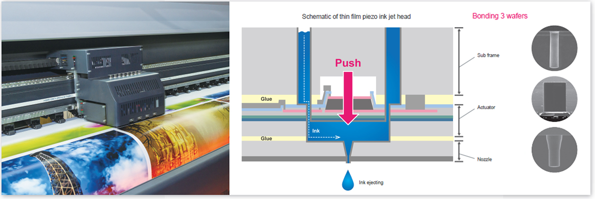
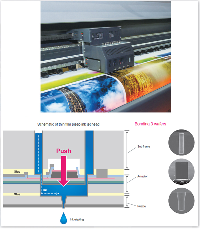
Thin film piezo inkjet head
LAPIS Semiconductor Miyazaki manufactures thin film piezo inkjet heads using PZT (lead zirconate titanate).
We use many MEMS technologies such as Si deep trench technology that requires high precision and bonding technology to bond three substrates.
This head is mainly applied to industrial inkjet printers.
Application