-
Solution
-
WL-CSP Structure
and Characteristic -
WL-CSP New
Technology -
Reliability Data
Services
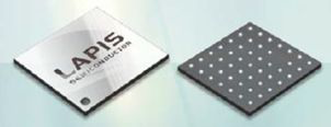
WL-CSP
Very small, thin package for smart phone/wearable
○Mold Type: Passed AEC-Q100 “G0” grade reliability test, and 18 years experience for automobile application
○Mold-less Type: Low profile 0.2mm Max. package height, 0.1mm fine pitch terminals
○Turn-key solution: RDL ~ singulation ~ electrical test ~ T&R packing
Cu RDL
Good solutions for power devices / high frequency devices
○Protect wire bonding damage by 15um thick RDL
○20% reduction of ON resistance compared with non-RDL
○Passive devices (inductor coil, etc.) with multilayered RDL
○High pin count with multilayered (2~3) RDL
Multi-Chip WL-CSP
Next generation package
○Multi-Chip structure by collaboration of RDL, Cu pillar and assembly technologies
○Low resistance due to short wiring compared with wire bonding connection
| Mold type | Mold-less type | |||
| Structure | 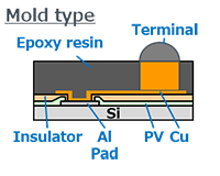 |
 |
 |
 |
| Features | High reliability (AEC-Q100 G0) |
Low-profile Fine pitch |
For device embedded substrate |
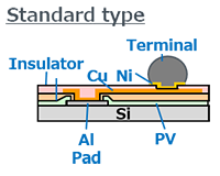
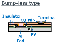
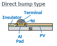
Terminal forming on Al pads |
| PKG height(total) | 0.3mm~ | 0.2mm~ | 1.6mm~ | 0.2mm~ |
| Terminal pitch | 0.3mm~ | 0.1mm~ | - | 0.1mm~ |
| Terminal diameter | 150um~ | 75um~ | 75um~ | 75um~ |
| Terminal height | 60um~250um | 20um~250um | 6um~ | 20um~250um |
Options: Backside treatment (resin coating, mirror finish), Plating (SnAg, Au, Ni)
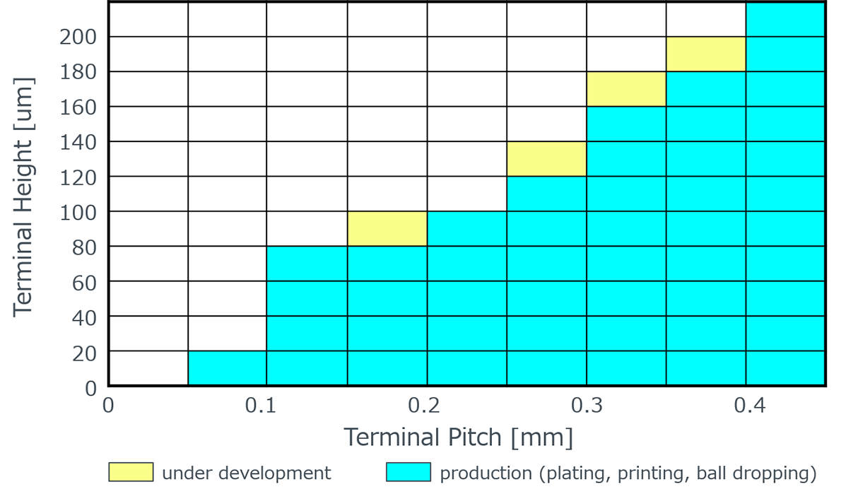
Terminal pitch / terminal height variation matrix
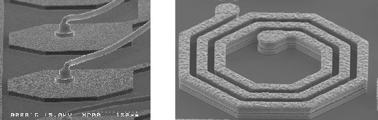
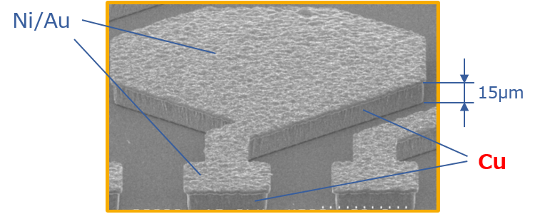
Thick RDL technology
Structure
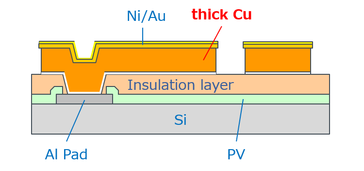
Cu/Ni/Au thickness * : 15/3/0.5μm
* standard Cu thickness: 5μm
Cu Line & Space : 30/30μm
Feature
Protect wire bonding damage by 15um thick RDL
20% reduction of ON resistance compared with non-RDL
30% chip size shrink with POE (Pad ON Element) structure compared with non- POE
Multi-layer Cu RDL technology
Structure
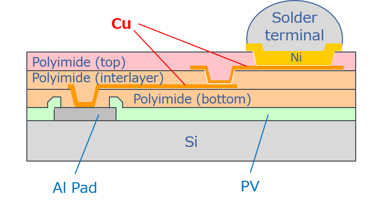
Cu RDL :5μm
# of Cu layers :2~3
Polyimide :13μm
Cu L/S : 30/30μm
Feature
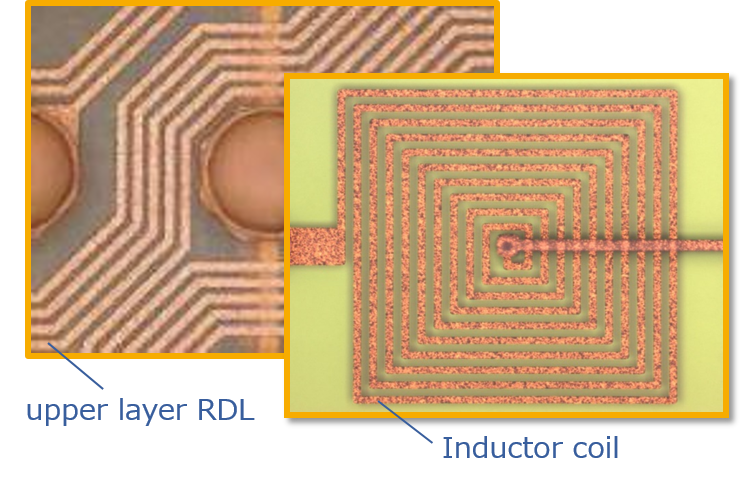
Embedded inductor coil by 2 layers RDL
High pin count with multilayered (2~3) RDL
Over 600V break down with 13um polyimide
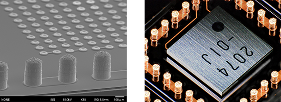
Multi-Chip WL-CSP technology
Structure
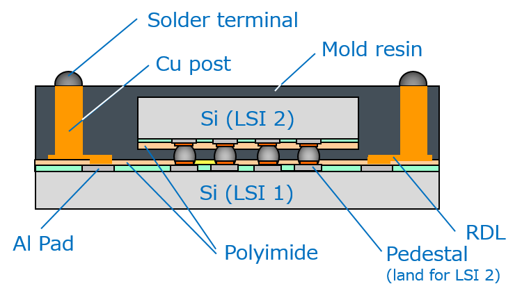
Cu RDL :5μm
PKG height :0.5mm Max.
Cu L/S : 15/10μm
Feature
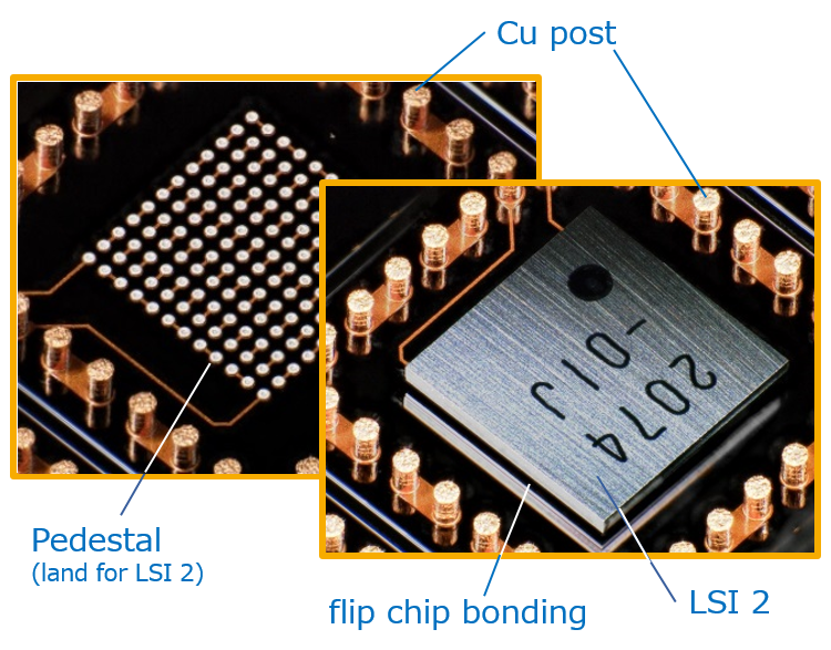
Chip-size MCP by 300µm high Cu post technology
Low resistance due to short wiring compared with wire bonding connection
Reliability data (AEC-Q100)
■Mold Type ~ Grade 0 ~
| Test Category | Test Condition | Note |
| Pre-condition | 85℃/85% RH, 168H, reflow 260℃ | Package Level |
| High Temp. Storage | Ta=150℃, 2000H | Package Level |
| Temp. Cycle | -65℃~RT~175℃, 500cyc | Package Level & Board Level |
■Mold-Less Type ~ Grade 1 ~
| Test Category | Test Condition | Note |
| Pre-condition | 85℃/85% RH, 168H, reflow 260℃ | Package Level |
| High Temp. Storage | Ta=150℃, 1000H | Package Level |
| Temp. Cycle | -65℃~RT~150℃, 500cyc | Package Level & Board Level |
Services
○RDL layout design, photomask preparation
○Pb-free soldering (plating & paste printing & ball mounting)
○Wafer mapping (generating and merging data)
○Full turnkey solution
・RDL ~ Insulation layer ~ terminal forming
・Singulation
・Electrical test (logic & analog)
・Die inspection (6D)
・Tape and reel packing
・Options / Si backside treatment (resin coating, mirror finish), plating (SnAg, Au, Ni)
○Ship to customer in wafer form, T&R
Drop ship to final customer