-
Outline of MEMS Foundry
-
MEMS Technology
-
Process and Equipment
| Location | Kiyotake-cho, Miyazaki-shi, Miyazaki prefecture, Japan |
| Clean room | 1360m2(MEMS dedicated area) |
| Clean rating | Class 100 |
| Wafer size | 6 inch |
| Production capability | Small volume engineering samples - Mass production |
| Services | Engineering samples, Production |
| ISO | ISO9001, ISO14001 |
| Development/ Production experience |
Actuator, Sensor |
| Process technology | PZT piezoelectric thin film, Bulk/surface MEMS processing, Double-sided Si processing, Wafer bonding |
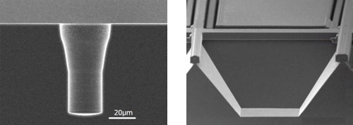
1. Si etching/through-hole and wafer surface processing
DRY etching
- Minimum width: 0.4μm
- Aspect ratio: up to 25
- Taper angle : 90±1 degrees
- Etch rate uniformity within a wafer: 5%
- Dimensional accuracy: ±0.1μm
Anisotropic Si wet etching
- Etch rate uniformity to depth within a wafer : 5%
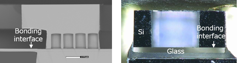
2. Wafer bonding/3D structure formation using wafer bonding
Resin bonding
Three wafers are able to be bonded by using resin bonding.
- Alignment accuracy: ±5μm
- Resin thickness: 1- 3μm
Glass anode bonding
- Internal pressure after sealing between Si and glass :>0.01Pa
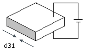
3. PZT technology/Sol-gel PZT with world-class piezoelectric property
PZT film has highly (100) orientation by the optimization of formation condition of sol-gel.
The PZT crystal orientation largely affect piezoelectric constant.
- Piezoelectric constant d31:-260 pm/V
- Film thickness uniformity within a wafer: ±1%
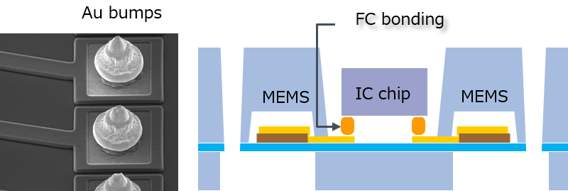
4. Flip chip bonding/Direct connection with Au bumps of flipped IC chip onto substrates
The advantages are:
- Reduced electric resistance between IC chip and substrates
- smaller package footprint
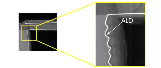
5. ALD/Atomic Layer Deposition
Thin-film deposition technology that uses sequential, self-limiting thermal reactions.
The features are :
- Excellent step coverage: ≒ 100%
- Film thickness uniformity within a wafer: 5%
ALD has capability to form hydrophilic or hydrophobic thin-films.
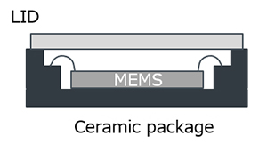
6. Vacuum package/Vacuum sealing in package
Useful vacuum sealing for IR sensor, motion sensor and RF switch.
The vacuum sealing consists of getter, lid and ceramic package.
- Getter enclosed in package to keep vacuum
- AuSn or solder sealing between lid and ceramic package in vacuum
- Si or Ge lid are available for IR transmission
| Process | Equipment |
| Photo lithography | Resist coater, Developer |
| Aligner, Double-sided aligner | |
| i-line stepper | |
| Deposition | Sol-gel(PZT) |
| AP-CVD(SiO2, doped-SiO2) | |
| PE-CVD(SiO2, SiN) | |
| LP-CVD(SiO2, Si2N3, poly-Si) | |
| Metal-CVD(W) | |
| Furnace (Thermal oxide, Thermal anneal) | |
| Sputter(Al-alloy, Au, Ti, TiN, TiW, Pt, Ir) | |
| ALD(Al2O3, SiO2, Ta2O5) | |
| Implant | Implanter(B, P, As, Ar, Si) |
| Planarization | CMP, Back-side grinder, Back-side etcher |
| Tape lamination | UV tape. Thermal release tape, PI film etc. |
| Dry etching | Si Deep RIE |
| Interlayer dielectric RIE | |
| Metal etcher | |
| PZT/Electrode ICP etcher | |
| Wet etching | Wet tools (SiO2, Au, TMAH) |
| Strip and Cleaning | Asher, Organic/Polymer stripper |
| RCA/Acid clean tools | |
| Wafer scrubber | |
| Wafer to Wafer bonding | Wafer bonder (Glue bonding, Anodic bonding with glass wafer) |
| Dicing | Wafer dicer, Jet cleaning including CO2 gas to prevent static charge |
| Circle-cut dicer | |
| Assembly | Vacuum sealer, FC bonder |
| Process | Equipment |
| Measurement | CD-SEM |
| Length measuring microscope | |
| Front and back misalignment measuring tool | |
| Microscopes (Optical, IR, Laser) | |
| XRD, XRF analyzer | |
| Laser displacement measuring tool | |
| Profile meter (Contact, Non-Contact) | |
| Ellipsometer, Film thickness meter, Sheet-resistance measuring tool | |
| Automatic visual inspection tool (AVI) | |
| Tr parameter tester, Auto-prober, Vacuum prober | |
| Analysis/Evaluation | Cross section SEM, SEM-EDX |
| FIB, Cross section TEM | |
| Optical microscopes | |
| Manual prober, Tester | |
| Contact angle measurement tool | |
| Ion milling | |
| Reliability tests at high temperature and for temperature cycle | |
| Electro-migration test |