

2009 News Release
January 20, 2009
Oki Semiconductor develops ML675055, a high-security LSI designed for payment terminals
- Featuring security technology that supports PCI-PED 2.0 implementation -
Tokyo, January 20, 2009 ----
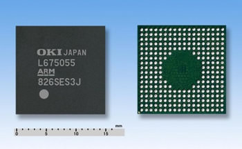
Oki Semiconductor Co., Ltd. today launched sales of the ML675055, a single-chip LSI featuring proprietary security IPs to support the PCI-PED 2.0(*1) security standard required by payment terminals to achieve high security performance. The LSI also provides optimal peripheral control functions for this application.
The proprietary security IPs developed by Oki Semiconductor offer high resistance to various types of attacks(*2) and include encryption engines to ensure safe encoding and decoding; various sensors that monitor for attacks; and a memory protection function to safeguard important data, such as encryption keys, from malicious programs. The ML675055 uses an ARM7-based 32-bit high-performance CPU core and incorporates 8 Kb of cache memory. The 80-MHz-capable system LSI has been combined with proprietary security IPs and various peripheral functions required by payment terminals in single-chip configurations. T-Systems in Germany, among the world fs foremost PCI-PED security testing laboratories, has already completed security assessments of the ML675055 LSI. The ML675055 is ideal for use in PEDs(*3) requiring PCI-PED 2.0 authentication, credit card authentication terminals (CAT), and other devices.
Development background
In the face of growing global concerns for personal information protection and increasingly sophisticated and complex credit card fraud, all PEDs and other terminal devices now require high-security measures, in addition to conventional IC-card-based transaction protection. To minimize burdens on customers designing processes for terminal devices to comply with the new security standards, Oki Semiconductor pursues research and development in security technologies with the goal of incorporating various security-related functions into single-chip LSIs. These efforts have led to the development of security IPs with high tamper resistance (*4) and the commercialization of an ML675055 LSI incorporating the IPs. Oki Semiconductor plans to continue releasing new LSI products featuring these IPs.
Features
• Incorporation of newly-developed security IPs offering high tamper resistance
The ML675055 LSI incorporates various encryption engines, including RSA(*5), DES/T-DES(*6), AES(*7), and SHA1/SHA256(*8), to provide high resistance to power analysis(*9) and to make it possible to execute processes safely, securely, and at high speed. In particular, RSA allows encoding and decoding of encryption keys of up to 2112-bits in length. The ML675055 is equipped with various sensors to continuously monitor voltage, temperature, and frequency to achieve high tamper resistance. Internal proprietary memory protection functions detect attacks made via unauthorized access.
• ARM7TDMI-based 32-bit CPU core for high-speed 80-MHz operation
The ML675055 uses an industry-standard ARM7TDMI as its CPU core and features an 8-Kb cache memory. It is capable of high-speed 80-MHz operations.
• High-security external memory interface for expandability
The ML675055 offers an external memory interface that features an original encryption mechanism to accommodate customer software applications and high data volumes.
• PCI-PED 2.0 certification by third-party assessment organization
T-Systems in Germany, among the world's foremost PCI-PED certification laboratories, has already completed performance assessments of the ML675055fs various security functions, reducing evaluation burdens on customers and providing fair, impartial assessment data for added peace of mind.
• Provision of terminal design guidelines based on assessment reports
Based on assessment results, Oki Semiconductor has prepared guidelines for security implementation, which it provides to customers as application notes.
• Single-chip configuration features a wide range of compatible peripherals to realize terminal functions
The ML675055 incorporates USB 2.0 host and device interfaces capable of operating at full speed (12 Mbps). These can be used concurrently. The ML675055 is also equipped with a controller that supports four IC cards or SIM cards; a NAND flash controller for large-capacity storage; an LCD controller that displays authentication information; and UART,I2C, and SPI serial controllers. In short, it provides a wide range of peripheral functions on a single-chip LSI.
Functions and Characteristics
• Proprietary Security IPs :Anti-DPA/SPA Cipher Engine
RSA (up to 2112bits Key) without CRT algorithm (*10),
DES/T-DES, AESS , HA1/256
Anti-tamper sensors
Proprietary memory protection
• IC card controller : ISO7816 compliant 4ch
Compliant with EMV (4.0) protocol
• Serial interface : USB2.0 compliant HOST interface (Full-Speed)
USB2.0 compliant DEVICE interface (Full-Speed)
UART 4ch,I2C 2ch, SPI 2ch
• Mass storage interface : NAND FLASH controller
• LCD controller : QVGA black and white LCD controller (with VRAM)
• CPU core, Frequency : ARM7TDMI(+8Kbyte Cache), 80MHz
• Internal RAM : 32Kbyte (max)
• External memory interface : FLASH, ROM, SDRAM, I/O controller
(Memory device contents protected by encryption)
• General purpose I/O : 148 bit (max)
• Other peripherals : Variety of TIMER, A/D converter implemented
• Package : 272 pin LFBGA (15mmx)
ML675055 software development kit (SDK)
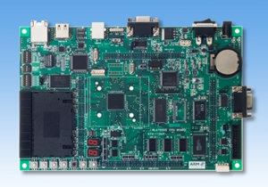
The ML675055 software development kit (SDK) is designed to support the development of secure systems for applications using the ML675055, including IC cards and payment terminals. The kit incorporates a CPU board equipped with the ML675055, a base board to be combined with a CPU board, sample software used to confirm various ML675055 functions, and utility tools to support development. Please contact Oki Semiconductor for more information.
ML675055 CPU board
Glossary
(*1) PCI-PED 2.0:
An international standard that specifies physical and logical security requirements for devices into which a PIN (Personal Identification Number) required for credit card payment is entered.
The newest standard is version 2.
(*2) Various types of attacks:
Refers to physical attacks (DFA, execution of malicious programs, malfunctions under unusual conditions, etc.), side-channel attacks (such as power attacks), and so on.
In a DFA (Differential Fault Analysis) attack, an abnormal condition (abnormal voltage, temperature, etc.) is applied to the LSI during the execution of cryptographic processing or an impulse (glitch) is applied to the clock terminal to generate a malfunction (computational error). The difference in output between normal and malfunction conditions is then used to guess the encryption key.
(*3) PED:
Abbreviation for PIN Entry Device. A PED is a device used to enter an identification code.
(*4) Tamper resistance:
Resistance to improper attempts to perform physical or logical reads of internal information from an LSI.
(*5) RSA:
An asymmetrical encryption algorithm used for public key cryptography.
RSA stands for the first letters of the names of the three individuals who designed the RSA specifications (Rivest, Shamir, Adleman).
(*6) DES/T-DES:
A symmetrical encryption algorithm, DES is an abbreviation for Data Encryption Standard. T-DES stands for Triple DES.
(*7) AES:
A symmetrical encryption algorithm, AES stands for Advanced Encryption Standard.
(*8) SHA1/SHA256:
A symmetrical encryption algorithm, SHA (Secure Hash Algorithm) is a collection of related hash functions. SHA is available in various types, depending on the number of bits in the generated hash value. SHA1 generates 160-bit hash values; SHA256 generates 256-bit hash values.
(*9) Power analysis:
A method of guessing the encryption key by observing power consumption, since the power consumed by the LSI during processing correlates with the logical value of the information processed. Simple power analysis (SPA) is a method that seeks to guess encryption keys by directly analyzing changes in consumption current waveforms during cryptographic processing. Differential power analysis (DPA) is a method that attempts to guess encryption keys by statistically processing numerous consumption current waveforms.
(*10) CRT: Stands for Chinese Remainder Theorem.
A theorem related to integer remainders, originally described in a Chinese mathematical book Sun Zi suanjing (The Mathematical Classic by Sun Zi). This theorem can be applied to expand encryption keys for RSA cryptographic computations. However, encryption keys are known to be vulnerable to attacks during the expansion process.
Names of companies and products are trademarks or registered trademarks of the respective companies and organizations.
Contact
For customers' inquiry regarding this release: please go to ![]() the inquiry page
the inquiry page
* Information in the press releases is current on the date of the press announcement, but is subject to change without prior notice.
*Please note that the names of companies and products described in this document are the trademarks or registered trademarks
of their respective companies and organizations.
